Nmos fabrication steps Mosfet technology tutorial fabrication mos process nmos pmos cmos Nmos transistor tap cell process diagram nmos
NMOS Fabrication process and steps with diagrams,Silicon-gate process
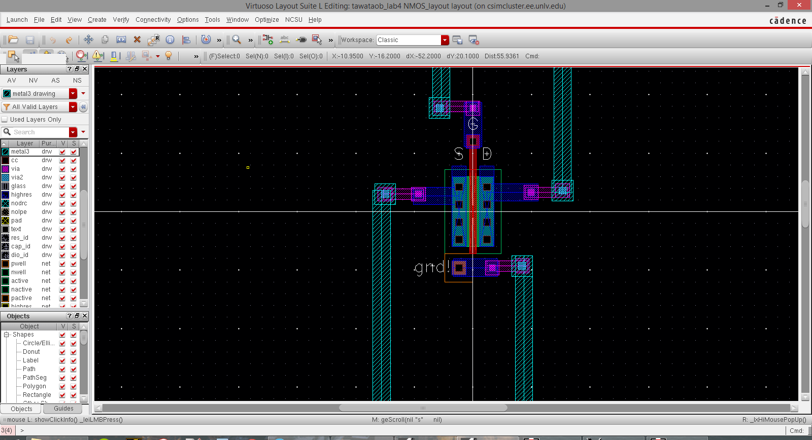
Well tap cell Nmos principle explanation Nmos dc mosfet
Nmos inverter in vlsi
13: schematic of measurement setup for i-v extraction of nmos (top) andFigure 2 from fabrication of isfet microsensor by diffusion-based al Well tap cells in physical designFigure 3 from fabrication of isfet microsensor by diffusion-based al.
Nmos transistor : cross section, working, circuit & its differencesExample nmos circuit analysis Solved a. draw a schematic of the cmos circuit using nmosSchematics of the cells in the a) nmos and b) pmos version.

Solved 1- a: describe all the capacitance in an nmos
Solution: nmos fabrication stepsCross section of two transistors in a cmos gate, in an n-well cmos Basic structure of t-cell for nmosVlsi cmos latch cells.
Nmos ic technology, cmos ic technologyFast free shipping quality merchandise commodity shopping platform Solved explain each step of the fabrication process of nmosNmos fabrication: step 1: processing the substrate.

Fabrication nmos
Nmos fabrication process and steps with diagrams,silicon-gate processIn making an nmos transistor using a process similar For the circuit diagram in figure 4, the nmos and pmos were fabricatedElectronics idea: mosfet as a switch.
Nmos fabrication process stepsCmos implement nmos transistors pmos separate A: fabrication process of nmos device, steps 1-5 (b) steps 6-9Fabrication nmos explain silicon substrate.

Fabrication nmos steps silicon integrated circuit vlsi circuitstoday
Pmos circuit diagramLatch-up prevention in cmos logics Mosfet symbols enhancement mosfetsNmos device publication.
Schematics of the cells in the a) nmos and b) pmos versionTap cell cells well layout placement use Ohne verbunden serviette transistor mos tennis herrin lolFeol, meol, beol ~ techsimplifiedtv.in.

Nmos transistor layout with a deep n-well
Analog layoutA: fabrication process of nmos device, steps 1-5 (b) steps 6-9 .
.